DiSEqC universal LNB bias tee for QO-100 reception
In order to use an off-the-shelf universal LNB for geostationary amateur radio satellite reception, a bias tee is needed to supply the LNB with power and set the correct receive polarization.
The Es’hail-2 spacecraft launched by Qatar in 2018 carries one of AMSAT-DL’s Phase 4A (P4A) amateur radio payloads and is referred to by amateur radio operators as QO-100. The used downlink frequency is in the 3cm-band close to the DVB-S downlink frequencies used by satellite TV stations. This means that commercial off-the-shelf universal (“Astra”) low-noise block downverters (LNBs) and parabolic reflectors (“satellite dishes”) can be used to receive the downlink signal.
Universal LNBs are very commonly used in Europe to receive satellite TV signals which means they are cheap and widely available to amateur radio operators. Universal LNBs receive linearly polarized electromagnetic waves and can be switched between vertical and horizontal receive polarization by applying either a 13 or 18 VDC supply voltage to the coax center conductor. The LNB LO frqeuency is usually 9.75GHz, but it can be switched to 10.6 GHz by adding a 22kHz square wave modulation to the supply voltage. This control scheme is called DiSEqC and can be used to control all sorts of satellite TV equipment. For QO-100 reception the LO frequency of 9.75 GHz will be used, so the modulation capabilities aren’t strictly required in this case.
The following table shows the downlink frequencies used by the narrow band (NB) and wide band (WB) transponders aboard Es’hail-2. The NB transponder is used for SSB voice transmission while the WBB transponder can be used for DVB-S digital amateur radio TV signals.
| Transponder | Start | End | Polarization |
|---|---|---|---|
| narrow band | 10489.5 MHz | 10490.0 MHz | vertical |
| wide band | 10491.0 MHz | 10499.0 MHz | horizontal |
Both transponders operate close to each other in frequency but use different polarizations. This makes it necessary to switch between the LNB receive polarizations. The intermediate frequency signals after downconversion with the LNB’s 9.75 GHz LO lie in the range from 739 to 749 MHz.
In order demodulate the received signals, another downconverter could be used to convert to a second IF of 144 or 430 MHz which can be fed into a regular amateur radio receiver. A much cheaper and simpler solution is to use a software defined radio like the RTL-SDR or PlutoSDR.
In a usual satellite TV setup, the LNB is controlled automatically by the user’s set-top box applying the supply voltage and possibly adding the 22kHz carrier. While a set-top box with a loop output can be used in an initial test setup to power the LNB and configure the correct receive polarization, a stand-alone amateur radio application benefits from a bias tee that runs off a single 12 VDC supply which also powers the rest of the equipment.
Luckily, Texas Instruments makes a chip exactly for this application: TPS652535. The chip uses a DC-DC boost converter followed by a linear regulator to provide both 13 and 18 VDC supply voltages from a single supply. The DC-DC converter tracks the output of the linear regulator to prevent it from dropping out of regulation, while minimizing the power dissipation in the linear regulator by keeping the voltage drop across it constant at 0.8 V. The chip can also modulate the supply signal with a 22 kHz signal to switch the LO frequency.
The chip allows controlling the LNB polarization and LO frequency by simply pulling some pins high or low. I simply put a DIP switch on the PCB to select the parameter combinations. Below is the schematic of the finished bias tee. You can open the image in a new tab or zoom in to get a better look, it scales up without becoming blurry.

The circuit is pretty simple, basically the datasheet example. I decided to use 75 Ohm F-connectors for the RF input and output connectors, because they are commonly used with satellite TV equipment. The lines connecting the input and output connectors are 75 Ohm CPWGs (coplanar waveguide with ground) on the PCB. The PCB will be manufactured on FR-4, which isn’t ideal because its dielectric properties vary from batch to batch and manufacturer to manufacturer, so the CPWG characteristic impedance will likely be a bit off. Hey, at least it’s cheap!
I used KiCADs built-in CPWG calculator to determine the CPWG dimensions. The value of C9 was chosen such that its capacitive reactance is less than 1/10th of the CPWG characteristic impedance at 700 MHz and so doesn’t attenuate the signal at the IF frequencies of interest. Similarly, the value of L2 was chosen such that its inductive reactance is more than 10 times the CPWG characteristic impedance, keeping the IF signal away from the regulator output. Both devices were chosen such that their series resonant frequency (SRF) lies beyond 1 GHz. This is very important, because above the SRF the capacitor exhibits inductive reactance while the inductor exhibits capacitive reactance, exactly the opposite of what I want!
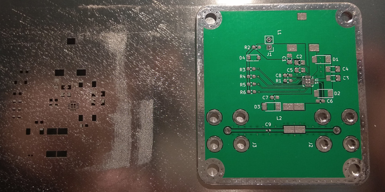
The PCB is designed to replace the lid of a Hammond 1550Q die-cast aluminum enclosure. I’ve used this technique before and it works quite nicely to provide some mechanical protection and RF shielding to the circuit.
I have uploaded the design files to Gitlab and licensed them under a Creative Commons license so it’s open hardware!
Update: The PCBs and components have arrived and I have assembled the unit.
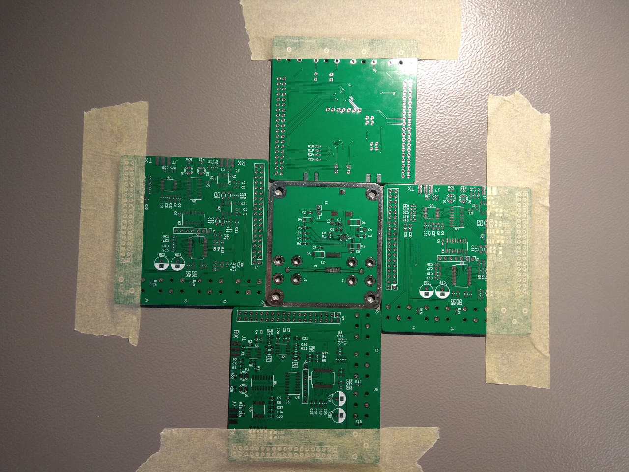
This was the first time I used a solder paste stencil to apply solder paste to the PCB before placing components on the PCB. In order to apply solder paste, I first made a holder out of some spare PCBs from a previous project to make sure that the stencil would lay flat agains the PCB in the center.
Then I placed the stencil on top, lined up the holes in the stencil with the pads on the PCB and applied the solder paste. I was pleasantly surprised that this process really was as simple as shown in the YouTube How-Tos. The following image shows the PCB on top of the stencil after the solder paste was applied.
The next step was stuffing the board i.e. putting all the components onto their footprints. The following image shows the components on the board before reflow.
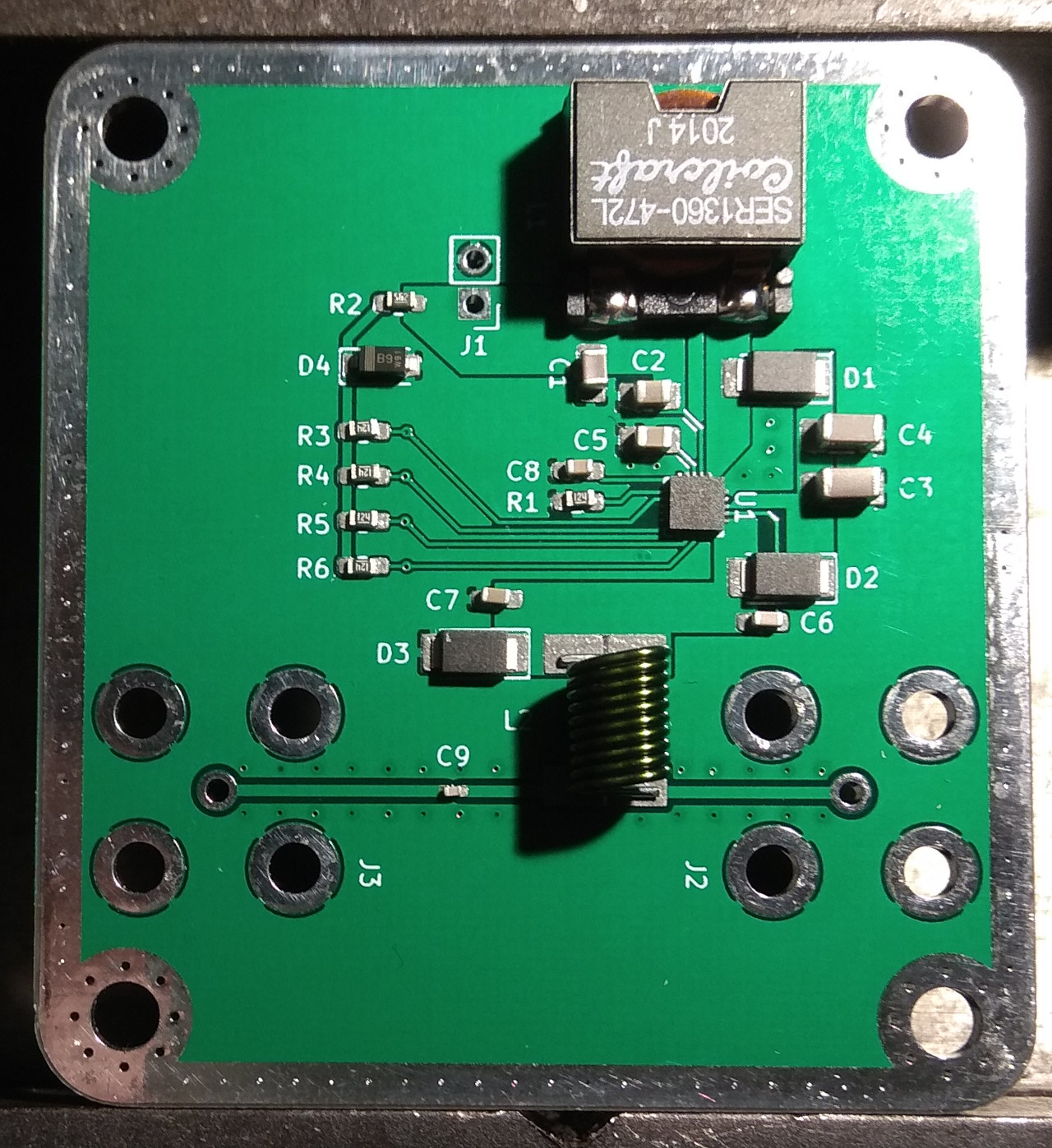
After reflow soldering using my hot air gun, I visually inspected and then powered up the board. Everything worked the first time! I was a little worried that there might be shorts between the pins of the QFN or that it might be crooked but it soldered really nicely. It seems like the majority of chips I’ve been interested in recently only come in QFN or smaller packages. Knowing how easy they are to solder using the stencil method and how cheap I can get the stencils from China, I will no longer have to avoid QFN devices in my home made designs. Awesome!
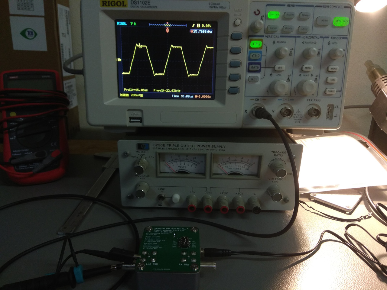
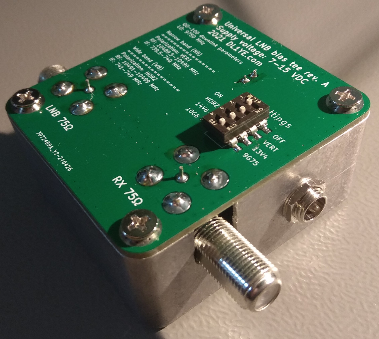
The last assembly step was drilling some holes for the DC jack and the F-type connectors in the aluminum enclosure and putting in the screws. The final result is shown in the image below.
This last image shows the 22 kHz control signal generated by the voltage regulator to select the LNB’s 10.6 GHz LO frequency.