28.8 MHz RTLSDR TCXO
A temperature compensated crystal oscillator for the popular RTL-SDR
This project was originally posted on hackaday.io
Description
The standard RTL-SDRs (and especially ones in a smaller case) drift quite a lot in frequency until they have warmed up. This makes receiving narrow band signals (for example in the HF bands using an upconverter) quite hard without periodically readjusting the tune frequency. A simple fix to this problem is using what is called a temperature compensated crystal oscillator (TCXO). I decided to use an off-the-shelf 19.2MHz TCXO, which is an easily available frequency normally used for WiFi or GPS applications.
The problem with the oscillator circuit that drives the R820T(2) tuner and RTL chipset is, that it operates at a frequency of 28.8MHz, which is a non-standard frequency and not easily available from popular electronics distributors.
By using a 19.2MHz oscillator and dividing that frequency by 2 using a 74AC74 D-type flip flop we can generate a 9.6 MHz square wave that contains a significant amount of odd-order (3rd, 5th, 7th etc) harmonics of the 9.6MHz fundamental frequency. By using a bandpass filter to filter out the 3rd harmonic of 9.6MHz, the needed signal at a frequency of 3 * 9.6MHz = 28.8MHz can be obtained.
Schematic
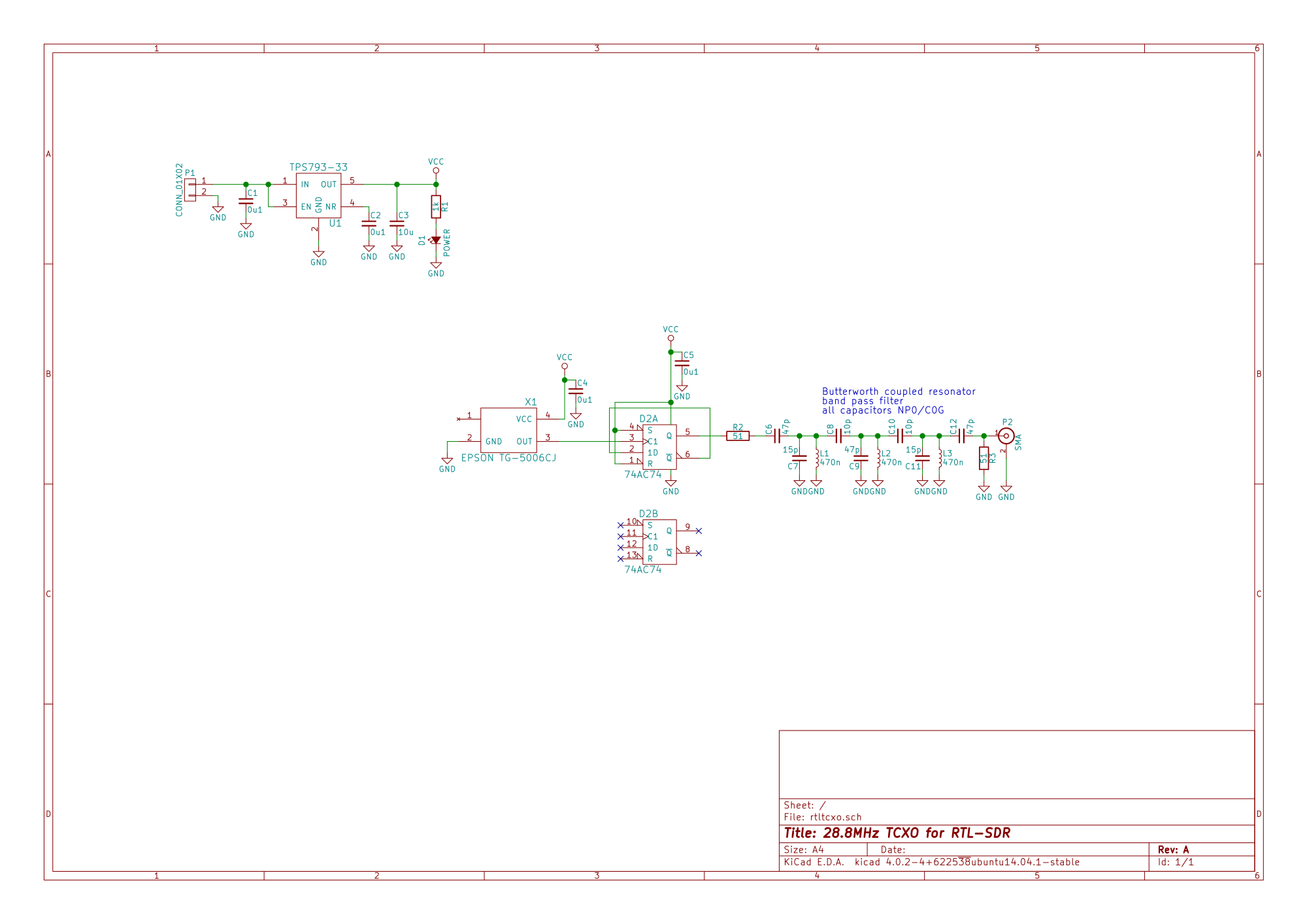
The circuit is super simple and doesn’t need a lot of further explanation. I added a 3.3V low noise LDO from TI and made the PCB as wide as the PCB in the RTL-SDR. This meanst that the can PCB be mounted on the backside of the RTL-SDR and allows the original case to still be closed.
The PCB also allows for an edge-launch SMA connector to be soldered in place which could be useful for building an external TCXO.
Hardware
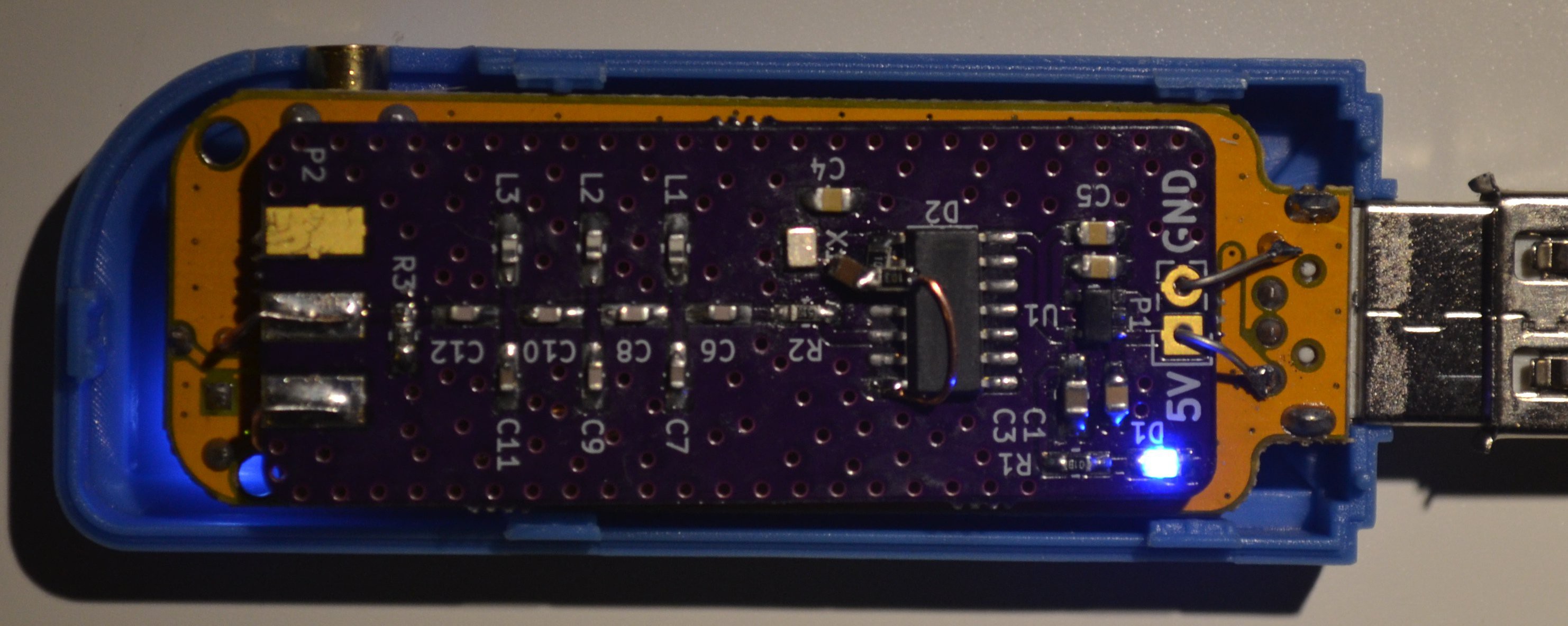
As you can see I did have to add a bodge wire to the circuit. The problem is that the output of the TCXO is only about 1V peak-to-peak, which is not enough to trigger the clock input of the D flip flop. The bodge adds two 10k biasing resistors to the clock input of the 74AC74 and the TCXO signal is AC coupled to the clock input via a 4.7uF capacitor. I had actually thought of this when doing the schematic, but somehow I was under the impression that the output amplitude of the TCXO would be high enough after looking at the datasheet. I probably misinterpreted the amplitude given in the datasheet.
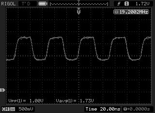
The image below shows the waveform on the clock input of the 74AC74 at 19.2MHz, you can see the 1.7V offset and the 1Vpp TCXO signal:
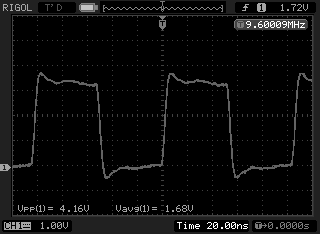
The output of the 74AC74 looks a little less pretty, with some overshoot on the rising and falling edges. I couldn’t get rid of that even probing with the little springy grounding tip:
And finally the 28.8MHz output after the band pass filter:
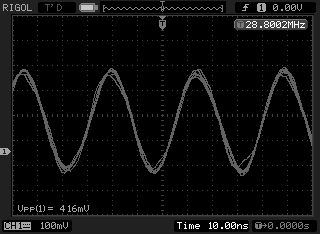
The output signal has quite a bit of jitter and you can clearly see that there are still higher order harmonics contained in the signal. It still kind of looks like a triangle wave with rounded corners rather than a pure sine, but it seems to work fine at least after a quick test. The dongle is also fine with the 400mVpp input signal, which according to the R820T datasheet is in the specified range of 150mVpp to 3.3Vpp.